The theory behind multicarts isn’t too complicated, and there are many ways of going about making them. Making multicarts for the classic retro systems is easiest when you use the reset button on the console to change games. There are some multicarts I’ve seen that have menus built-in (I mean, technically, Mario Bros/Duck Hunt was a multicart with a menu at the start) but this tutorial will not be going over how to make and use those. Besides, this site is more hardware based, rather than software. Perhaps in the future there might be a section about that, but for now, let’s go into some simple circuitry you can use to put multiple games on one cartridge.
This article is mostly going to explain things in a general sense, rather than specific to one console. But if you can read through this and understand it, you should be easily able to generate your own circuitry to make a multicart. There are two main ways that I use to make multicarts. There are definitely other was of doing this, but these are the easiest to understand and use in my opinion. The first, and easiest, is using a simple flip-flop to switch between two ROM chips, or two memory chunks on one chip, to make a 2-game multicart. The second more complex method is using a binary counter to cycle through memory addresses on one ROM chip to potentially put more than 2 games on one cartridge.
The Flip-Flop
A flip-flop in the most basic sense is a device that can change an output between an ‘on’ state and an ‘off’ state based on various inputs, and is generally used as a “memory cell device,” or a device that holds a bit of memory (either 0 or 1) without reacting to the input until called upon. There are various types of flip-flops with different features, but for the sake of this article, we’ll be looking at the “D flip-flop”. The ‘D’ stands for ‘data’. Check out a single D flip-flop cell below.

Here we see six different pins: D, >, S, R, Q, and ‘Q bar’ (henceforth denoted as /Q). The functions of these pins are pretty straightforward.
D : Data input
> : Clock input (CLK)
S : Set
R : Reset
Q : Data out
/Q : Inverse data out
First, let’s go over how the data, clock, and data out pins relate to each other. We can see how they affect each other based on this simplified truth table.
| D | CLK | Q | /Q |
| 0 | Rising Edge | 0 | 1 |
| 1 | Rising Edge | 1 | 0 |
| X | Not Rising Edge | Q | /Q |
You can see from this table that the output Q becomes whatever is on the input D when the clock changes from low to high (or, the rising edge). When the clock signal is not moving, or if it falls from high to low, the Q and /Q outputs stay exactly what it was, no matter what the D pin is doing. The output therefore only updates to the input whenever the clock signal rises from low to high. And, if you hadn’t guessed already, /Q is always the inverse of the Q pin. Here’s a quick timing diagram to help explain the truth table. Note that only when the clock has a rising edge, does the state of the Q pins update to whatever we input to D at that time.

Now, the S and R pins. These pins basically override whatever is on the Data pin and forces the Q and /Q pins to a certain value. If they are both disabled, then the output follows the data pin based on the clock pin as described above. We don’t really use the S and R pins in this explainer, but here’s the truth table anyway.
| S | R | Q | /Q |
| 1 | 0 | 1 | 0 |
| 0 | 1 | 0 | 1 |
| 1 | 1 | 1 | 1 |
You can think of this as “when the chip is set, the output is 1” and “when the chip is reset, the output is 0”. Normally, you shouldn’t put S and R to both be true, but the D flip-flop can reconcile this by setting both Q and /Q high.
Note that for many flip-flops, like the 74HC74, the S and R pins are inverse logic – that is, they are actually /S and /R. This means that the truth table is inverted for both the S and R columns. Practically speaking, this just means we need to set these pins high in order to enable the flip-flop to operate normally.
Using the flip-flop as a toggle
Now that we’ve got an idea of how to use the flip-flop, we can use it for some more clever things. What if, instead of feeding the flip-flop data ourselves, we feed it it’s OWN output?
If we connect the /Q pin to the D pin, then every time the clock pin sees a rising edge, the D pin will flip from 0 to 1, or 1 to 0. Think about it like this (assume the D pin starts at 0):
Step 1: D is at 0.
Step 2: Clock pin sees rising edge.
Step 3: Q becomes whatever D was (0). /Q becomes the opposite (1).
Step 4: D becomes /Q (1).
Step 5: Clock pin sees rising edge.
Step 6: Q becomes whatever D was (1). /Q becomes the opposite (0).
Repeat.
So you can see that with this set up, the Q pins will toggle between 0 and 1 every time the clock pin is pulsed. The downside is, without some extra circuitry, we can’t control what the state is when the chip powers on. But this isn’t a huge concern for our purposes.
You can start to see how this toggling might be useful. What if we connected the clock pin to the /RESET line on the cartridge connector? The NES, SNES, and Genesis all have a variation of this line. This changes from 1 to 0 anytime the reset button is pressed, and back to 1 when the button is released. If we connect this line to the clock pin of the flip-flop, we’ve essentially created a toggle that changes state every time we let go of the reset button. So now, we just have to use this toggling signal between 0 and 1 to switch between two ROMs!
Toggling between two ROMs on one chip
For this explanation, I’ll use an 8 Mbit EPROM as an example. This chip can hold up to 1 MB (or 8 Mbit) of data. This is done with 20 address pins (A0 to A19). Each combination of address pins holds 8 bits of data. To prove the size of the chip, just do the simple calculation:
2^(number of address pins) * number of bits = size of chip
2^(20) * 8 = 8,388,608 bits (or, 8 Mbit)
Since 1 byte is 8 bits, dividing this by 8 yields the size in bytes.
You can visualize the data on a chip like it’s in a list. Each row is the address pin configuration, and the column is the 8-bit word contained at that address. Here’s a random assortment of data as an example. (To make it a bit easier on the eyes, I’ll list the data as a hexadecimal number).

It’s a bit clunky to look at, but you get the idea. See that I’ve split the table into two halves with the thickened border there. Let’s move the bottom half over to the side.
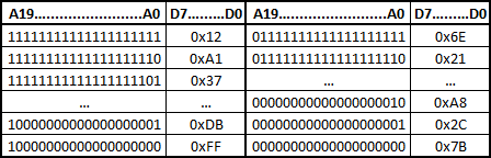
The left table always has A19 as ‘1’ and the right table always has A19 as ‘0’. See what I’m getting at here?

We then call the two sections of memory for A19 as memory “banks”. ROM1 and ROM2 are now two 4 Mbit sections of memory.
Practically speaking, this means you take two ROM files together that are each half the size of the EPROM or whatever memory chip you’re using, and stitch them together. Program them onto the chip, and then take the highest address pin, and connect it to the output Q of the flip-flop toggle circuit. That way, whenever you press the reset button on the console, the memory location will shift from one ROM to the other, and because the reset button causes the program to start over, you won’t encounter any weird glitches or skipping in the program. Pretty simple!
Toggling between two ROMs on two chips
Again, I’ll use 8 Mbit memory chips as a base example. The concept of this method is quite simple – all we have to do is connect one of the ROM chips to Q and the other to /Q, to make sure only one chip is enabled at a time. But where to connect those Q lines exactly, in order to enable each chip?
EPROMs, and flash memory, normally have two enable pins – chip enable (/CE) and output enable (/OE). Again note the bars before the pin name – these pins enable the chip whenever they are 0 (normally, GND). In order for a ROM chip to make output on the data pins, both of these enable lines must be driven to 0. If only one of them is 1, then output won’t be made on the data pins. When wiring the two ROM chips, all of the other pins, like the address and data and power pins, can be wired in parallel with each other – these pins just won’t do anything on a chip that’s disabled, so its ok to keep them connected.
Depending on the system you’re making a game for, these enable pins could be going to a number of different places. You don’t want to screw up or disconnect these pins unless you make sure it doesn’t ruin the correct operation of the ROM chip.
NES games, for example, commonly tie the /CE pin directly to GND, and change the /OE pin to control the output, instead of dealing with two signals. This is convenient – if we take the /CE pin out of the socket so that it’s not connected to GND, we can instead connect it to one of these Q outputs on the flip flop. Wire up a second ROM chip in parallel so they share all the same signals, except wire the second chip’s /CE pin to the other Q output, and you’ve now got two ROM chips that toggle whenever you press the reset button! Remember that many NES games have two ROM chips, so you have to toggle both of them simultaneously in order for it to work correctly.
Unfortunately, some consoles like SNES and Genesis, use both of these enable pins already. So in order to toggle between ROMs without screwing up the function of the ROM, we need to add some extra circuitry that basically ensures one of the ROM chips is always disabled. An easy way to handle this is with a decoder, like the 74HC139.
Toggling using a decoder
A binary decoder chip is pretty straightforward – it’s a very handy device, essentially taking a “binary” input and outputting a “decimal” result.

This is an internal diagram from a TI datasheet for the 74HC139. You can see the A and B inputs at the left – this is the “binary number” input into the device. Based on what this input is, one of the Y pins on the right is pulled to GND (assuming the VSS pin on the chip is also connected to GND). Y0 corresponds to a decimal 0, Y1 corresponds to a decimal 1, and so on. So, if you set A and B to both be 1 (which would be 11 in binary, or 3 in decimal) the Y3 pin would be pulled to GND. The /G pin is the enable pin, and it will force the output of the Y pins to be permanently high if it is not enabled. Here’s the truth table for the ‘139.
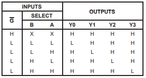
As you can see, when the /G pin is high, all the outputs are high, no matter what the A and B inputs are. And when /G is low, the chip is enabled, and the output can follow the binary input on the A and B pins.
Maybe you see the trick already. What we can do is connect the A pin to Q or /Q from the toggle circuit we made, and tie the B pin to GND permanently. So the A pin will drive the outputs Y0 and Y1 to alternate driving to GND (Y2 and Y3 won’t change at all). These two pins can be wired directly to the /CE pins on our two ROM chips. The original connection to the /CE pin on the ROM can be routed to the /G pin on the decoder instead. That way, whenever the console doesn’t want the ROM to output data, it’ll just disable the decoder chip, which will disable both ROM chips.
So now we know a few different ways to use flip-flops to make a two-game multicart. Neat! But what if we want… MORE than two games?
The Binary Counter
With a binary counter, you can put many more games onto one cartridge. The idea is similar to the section above where we used a flip-flop toggle circuit to switch between two data banks on one ROM chip. So if you skipped that part, go back and read it to get an idea of how the memory is organized.
All we’re going to do with the counter is connect the “counting” pins to the upper address pins of the ROM chip. As a new example, let’s use a 32 Mbit chip (4 MB) with an 8-bit data bus. This theoretical 32 Mbit chip has address lines that go from A0 to A21, for 22 total address lines.
2^(number of address pins) * number of bits = size of chip
2^(22) * 8 = 33,554,432 bits (or, 32 Mbit)
Confused why 33.5 million bits is still considered “32 megabits”? Check out this Wikipedia article!
If we use the top address line A21 as we did in the previous example, to toggle between two ROMs on the same chip, we essentially divide the ROM space by 2, and get two 16 Mbit memory banks. Each bank uses address pins A0 through A20 now. This is proven by the math here:
2^(number of address pins) * number of bits = size of chip
2^(21) * 8 = 16,777,216 bits (or, 16 Mbit)
But what if we do that again? Take the next highest address line and make two banks within these two banks? That’s a total of four memory banks, and since we removed one address pin…
2^(number of address pins) * number of bits = size of chip
2^(20) * 8 = 8,388,608 bits (or, 8 Mbit)
We now have four 8 Mbit ROM spaces. Expand this one more time, and you can get eight banks sized at 4 Mbits on one 32 Mbit ROM chip. The data will be organized into the banks shown here. Remember that the ROM spaces are filled with the 8-bit data at each address location, one 8-bit word for each row.

To make it easier to look at, let’s reduce the binary into hexadecimal, keeping in mind that the columns are defined by bits from A19 to A21 and the rows are defined by bits from A0 to A18. It might start looking familiar to those who have read my SNES explainer article!

So again, practically speaking, the data on the ROM chip would be made by taking eight 4 Mbit ROMs, all stitched together, and programmed.
Ok, so back to the binary counter. The counter, depending on its size, has a certain amount of binary “counting” pins, normally labelled Q0 to Qn (for example, for a 4-bit binary counter, n would equal 4). These pins increment every time the clock pin is pulsed (changes happen on the rising edge of the clock signal), and will increment to represent a binary number. This means (assuming we count from zero) that after the first clock pulse, Q0 would change from a 0 to a 1. The second pulse changes Q1 to 1, and Q0 back to 0. The third pulse changes Q0 to a 1, while keeping Q1 at 1. It’s just counting up a binary number! Once it reaches the maximum binary number it can count to, it restarts at 0. Using a 3-bit binary counter as an example, here’s a table and a timing diagram to help visualize.
| Number of clock pulses | Q2 | Q1 | Q0 |
| 1 | 0 | 0 | 1 |
| 2 | 0 | 1 | 0 |
| 3 | 0 | 1 | 1 |
| 4 | 1 | 0 | 0 |
| 5 | 1 | 0 | 1 |
| 6 | 1 | 1 | 0 |
| 7 | 1 | 1 | 1 |
| 8 | 0 | 0 | 0 |
| 9 | 0 | 0 | 1 |
| 10 | 0 | 1 | 0 |

Compare this table to the table we made earlier with eight banks of data. You might notice that Q0 lines up with A19, Q1 lines up with A20, and Q2 lines up with A21. So instead of routing these address lines to the console to control, we can route them to the binary counter’s Q pins instead. If we connect the clock pin to the reset line like we did earlier with the flip-flop toggle circuit, we have made a system that cycles through the ROM files on a single ROM chip every time we press the reset button on the console.
If you instead just wanted to put four 8 Mbit ROMs onto the chip instead of eight 4 Mbit ROMs, you don’t need to find a 2-bit binary counter either. You can just not use the Q2 pin on the 3-bit counter. The lower pins still count up and reset to 0 after reaching the fourth bank! A popular binary counter IC is the 74HC161 family of parts. This is a 4-bit binary counter. So for our eight-ROM example above, we would just use Q0 through Q2 and ignore Q3.
Conclusion
So now you’re equipped with a few different methods of making a multicart. There is one notable side effect of these very simple methods, and that is you cannot always know what state the logic chips are in when they are first powered up, without adding some extra circuitry to control it. The flip-flop might start with Q as a 0, or as a 1. In my experience with my design, the Q pin with the toggle circuit above usually starts up as a 1, which just means my second ROM is loaded first (so if I care about which game starts up first, I just flip the order the two ROMs are programmed). With the binary counter, it seems to load up as if it has already received a clock pulse, so the Q0 pin starts at 1 and counts up from there with each press of the reset button.
There are ways to mitigate these problems, like holding the /RESET pin on the ‘161 at GND for a bit before releasing it to allow the chip to function, but I find that it’s cheaper/easier to just program the ROMs so that the first game is in the second slot. I don’t normally care what order the games start up in anyway.
As with all digital logic circuits, there are many ways of designing a circuit to achieve the same goal, or to expand on that goal. I have a Sega Genesis board that uses both a flip-flop AND a binary counter, in order to get up to eight 8 Mbit games between two 32 Mbit chips on one cartridge! The possibilities are endless, and hopefully this serves as a good primer to understand the basics.
