Please look at the main entry for more information on how to prepare the ROM file!
Here’s a guide on how to populate my custom designed NES reproduction PCB. This board supports most MMC1 games with the SxROM board name (where the lowercase ‘x’ is a stand-in for other board types). This means you can make games that use boards like SLROM, SNROM, etc. Check out the Nesdev wiki entry on SxROM games here. The board can use an original MMC1 chip harvested from an NES game, and is also capable of using the AX5904 clone chip to imitate the MMC1 mapper.
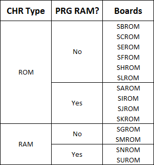
Here is a table of the various SxROM boards and their required hardware. Note that a few board types are not supported: SOROM, SXROM, and SZROM.
I’ll break down the different parts used for each kind of game here. Some ways you can find information about the game you want to make include using a tool like FamiROM, or possibly by looking it up on NesCartDB.
Top Side Parts
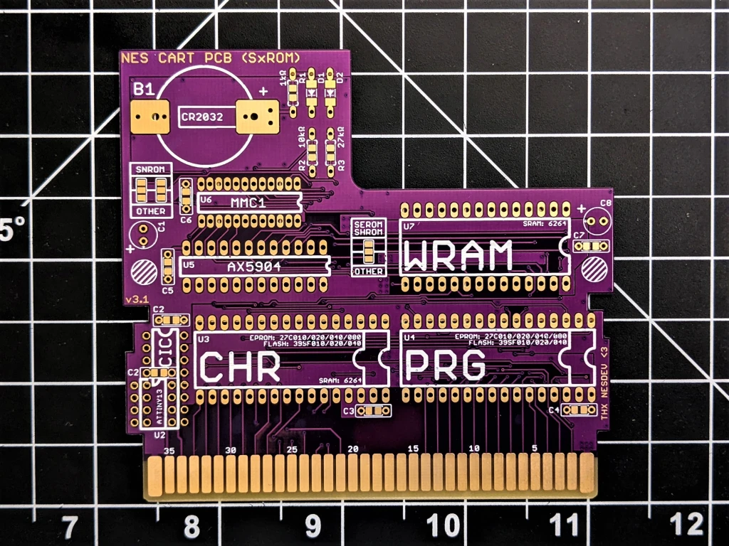

U4 – PRG ROM
Needed for: All game types
Part Number: EPROMs: 27C256, 27C512, 27C010, 27C020, 27C040, 27C080; Flash memory: 39SF010, 39SF020, 39SF040
Function: Holds the Program ROM file. This is placed in the socket marked PRG.
How to Program: Check the reproduction article for information (Steps 1, 3, and 4)
U3 – CHR ROM
Needed for: Most SxROM games, notably SLROM – check your board type using FamiROM
Part Number: EPROMs: 27C256, 27C512, 27C010, 27C020, 27C040, 27C080; Flash memory: 39SF010, 39SF020, 39SF040
Function: Holds the Character ROM file (sprite data). This is placed in the socket marked CHR.
How to Program: Check the reproduction article for information (Steps 1, 3, and 4)
U3 – CHR RAM
Needed for: A few SxROM games, notably SNROM – check your board type using FamiROM
Part Number: 6264 series
Function: Holds the ROM’s sprite data. This is placed in the socket marked CHR.
U7 – PRG RAM (WRAM)
Needed for: A few SxROM games, notably SNROM – check your board type using FamiROM
Part Number: 6264 series
Function: Used for normal operation of some games, and/or holds save data. This is placed in the socket marked WRAM. Note that some games use WRAM without utilizing save functionality.
U2 – CIC
Needed for: All game types (unless using a top-loader NES, modded NES, or clone console)
Part Number: Original CIC, or programmed ATTiny13 (instructions for programming provided below)
Function: Completes the region check and allows the game to run on the console.
U5 and U6 – Mapper
Needed for: All games (use either U5 or U6, not both)
Part Number: MMC1 (for U6), AX5904 (for U5)
Function: Used by the NES for memory management, allowing for increased memory size and features. Note that the AX5904 is not the original MMC1 chip, it is a clone chip that acts as a replacement for the MMC1 which is a proprietary chip designed by Nintendo. Some sources of AX5904 chips have been known to provide faulty parts from time to time, however any that I provide for purchase have been tested.
R1, R2, R3, D1, D2 – Resistor and Diodes
Needed for: Games that save
Value: 1kΩ for R1, 10kΩ for R2, 27kΩ for R3; low reverse leakage diodes (BAT85 or 1N4148) for D1 and D2
Function: R1 acts as a current limiting resistor from the battery supply to the RAM chip that holds save data. R2 and R3 are pull-down resistors for two pins on the mapper. Diodes combine the voltage from the NES and the voltage from the backup battery to power the RAM. To lengthen save data retention, it’s better to get diodes that have a low reverse leakage.
C1 – Electrolytic Capacitor
Needed for: All game types
Value: ~22 uF, at least 10 V rated
Function: Smooths out supply voltage for the board due to transients on the power supply, prevents quick changes in supply voltage when power is turned off.
C2, C3, C4, C5/C6 – Ceramic Capacitors
Needed for: All game types
Value: ~0.1 uF, at least 10 V rated
Function: Filters out high-frequency noise that can interrupt the EPROMs, SRAM, mapper, and importantly, the CIC. There are two places for C2, depending on the CIC you are using – you only need to use the one closest to the chip you use.
C7 – Ceramic Capacitor
Needed for: Games that have WRAM, notably SNROM
Value: ~0.1 uF, at least 10 V rated
Function: Filters out high-frequency noise that can interrupt the RAM chip.
C8 – Electrolytic Capacitor
Needed for: Games that save
Value: ~22 uF, at least 10 V rated
Function: Smooths out supply voltage for the board due to transients on the power supply, prevents quick changes in supply voltage when power is turned off. This is a contingency for preventing loss of save data.
CR2032 – Battery
Needed for: Games that hold save data
Value: CR2032 (socket is designed for yellow ones with pre-attached legs)
Function: Keeps the WRAM powered on after the NES is powered off to hold save data.
Top Side Solder Pads
There are five sets of solder pads on the board – two sets on the top, three on the back. Except for the battery bypass solder pads on the back, you must bridge these solder pads on every game in the proper setting. To choose a setting, simply add solder across the middle pad to the left/right or top/bottom depending on the pads, and depending on the setting you require. Be sure not to accidentally solder all three pads together.
SNROM Enable
Solder the middle two pads to the top if you are making an SNROM game. If you are not, solder the two middle pads to the bottom setting, labeled “OTHERS.”

SHROM/SEROM Enable
Solder the middle two pads to the top if you are making an SHROM or SEROM game. If you are not, solder the two middle pads to the bottom setting, labeled “OTHERS.”

Back Side Solder Pads

CHR ROM/RAM Solder Pads
Solder the middle three pads to the top if you are making a game that uses CHR ROM, or to the bottom if you are making a game that uses CHR RAM.

Battery Bypass Solder Pad
This solder pad bypasses D2 for games that don’t hold save data, but use PRG RAM (WRAM). Only solder this if you are using WRAM without a back-up battery. If you solder this with a battery on the board, it will drain the battery power quickly. You do not need to solder this if your game does not use WRAM, but soldering it won’t cause any problems.

Flash/EPROM Solder Pads
Solder the middle pads to the left if using Flash memory (39SF series) for the PRG ROM chip. Solder to the right if using UV EPROMs (27C series) instead.

Backside Components
In rare cases, you might encounter some sprite glitching even if everything is configured properly. This usually only happens when you have things like a Famicom-NES adapter or Game Genie in your system. What sets this aside from other graphical glitches is that it affects the sprites, not the entire screen. So if you’re getting strange palettes, missing backgrounds, or weird tiles, your problem is something else, probably a bad cartridge connector or dirty cartridge edge. What you’ll see if you’re getting this kind of error, known as OAM corruption, looks something like this:
Fixing this error involves adding ~100 ohm resistors in series with the PRG D0 to D7 lines. This can be done by cutting the exposed traces in the middle of RD0 to RD7 with a blade, and soldering resistors in place (surface mount size 0603). Be careful not to cut other parts of the board (or yourself).


Again, this is quite rare, so chances are you will be leaving these alone.
Programming the CIC
The CIC clone by krikzz uses the ATtiny13 microcontroller. You need an AVR programmer to properly load the program into the chip. You can use the GQ-4×4 or the TL866.
In order to program the ATtiny13, first load up the chip in the programmer, and load the code found here (I could not find the original file uploaded on kirkzz’s website, but you should still check out his stuff). Make sure you load the .hex file, and load it in as a .hex file. The ASCII code on line 0x380 should read “krikzz was here!” – that’s how you know it loaded correctly.
If you’re using the GQ-4×4, first write the software to the chip, and then set the config bits – so program the chip first. If you’re using the TL866, you can write the code and the config bits at the same time. To set the config bits, hit “CFG” for the GQ-4×4, or the “Config” tab on the right of the screen for the TL866. Then, set the bits like this:


Hit “Write” for the GQ, or program the chip on the TL866, and then you should be good to go!
When you put it into a cartridge and load it on the NES, you will probably need to hit the reset button five to ten times to get it to recognize the region of the NES you’re using. If you happen to use the cart in another region NES, just do this reset process again to reset the region correctly.

[…] Mapper Guide MMC1 Mapper Guide MMC3 Mapper […]
LikeLike