These two boards house the 32 Mbit 27C322 EPROM or the 16 Mbit 27C160 EPROM to fit in donor SNES boards or custom SNES PCBs. This saves you a TON of time adding wires to your board, and comes with the added benefit of not having to remove the original ROM from the donor board.

NOTE: When put into the board properly, these boards should fit nicely inside the cartridge. They will not fit inside the cartridge on every existing SNES board. There must be at least approximately 2 centimeters clearance to the top of the cartridge. In general, if your board only has one ROM and SRAM chips, or two ROMs and no SRAM, it should fit ok. You might need to clip a bit of the plastic structure inside the cartridge to get the board to fit, but it won’t show on the outside of the cartridge.
There are two major versions of the 322 boards – one with surface mount parts, one with through-hole parts:

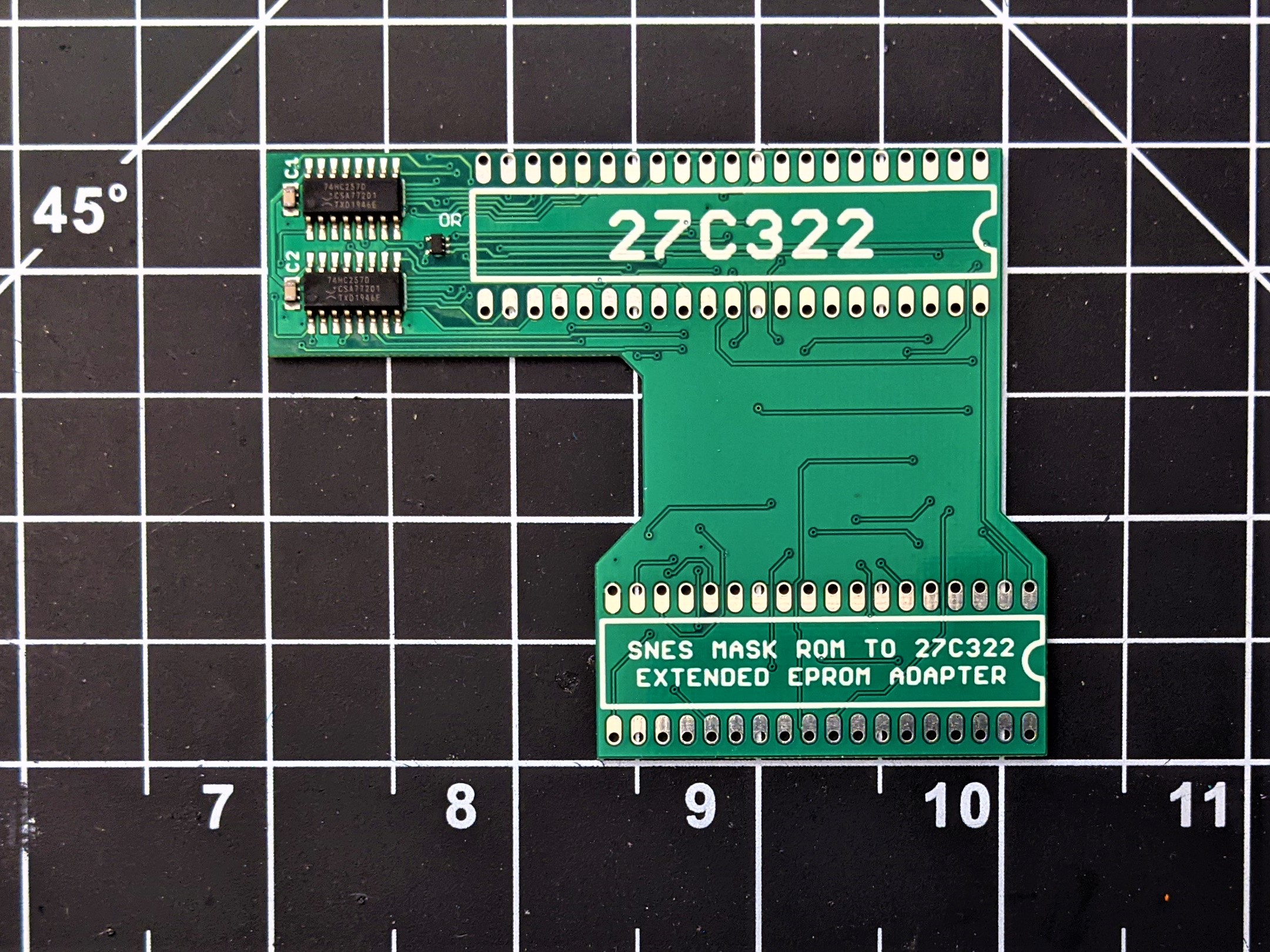
The 27C160 boards do not have any extra parts, other than the EPROM!

Here’s a better picture showing the clearance you need between the top of the board and the top of the cartridge.

How to Use the Adapters (36-pin Socket)
The first thing you should do is check out your donor cartridge. You’ll be putting the adapter board on the existing Mask ROM pins on the back of the board, but you might have some other chip, like SRAM, that the adapter might interfere with. Trim down any of those pins on the back to make sure the adapter board is as flush with the donor board as possible. Do not trim the pins on the ROM.

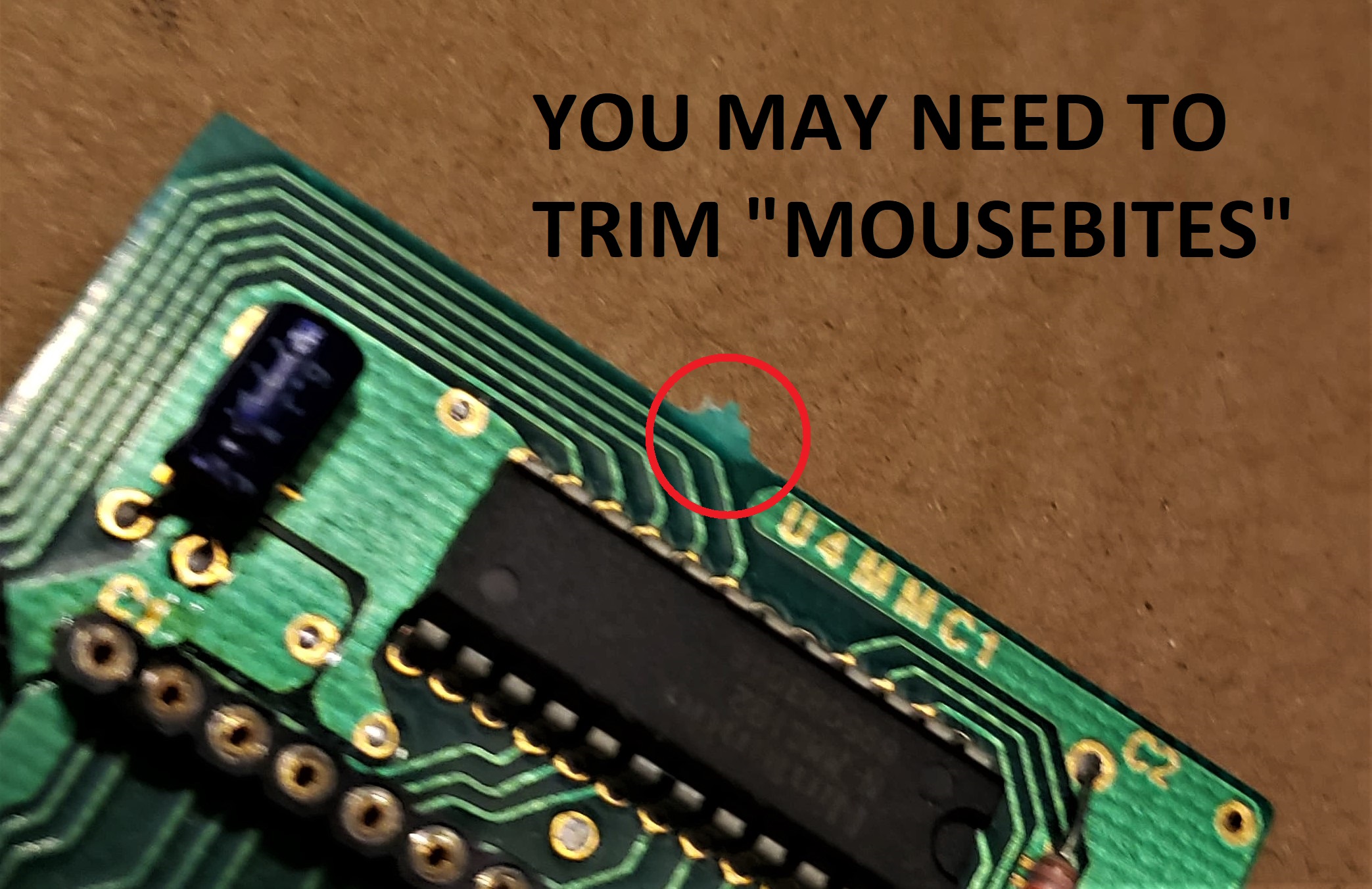
Also, there might be some little tabs on top of the PCB – these are called “mousebites”. They’re a left-over of the original board manufacturing, basically this board would be attached to another board at this point, and you would snap them apart (multiple boards connected to each other in this manner make up a “panel”). You might have to clip these back to fit the EPROM into the socket.
Now, you’ll want to solder the board onto the pins of the Mask ROM. Make sure you add enough solder so that it goes down into the holes and attaches to the pins, but not too much that some short to nearby pins.

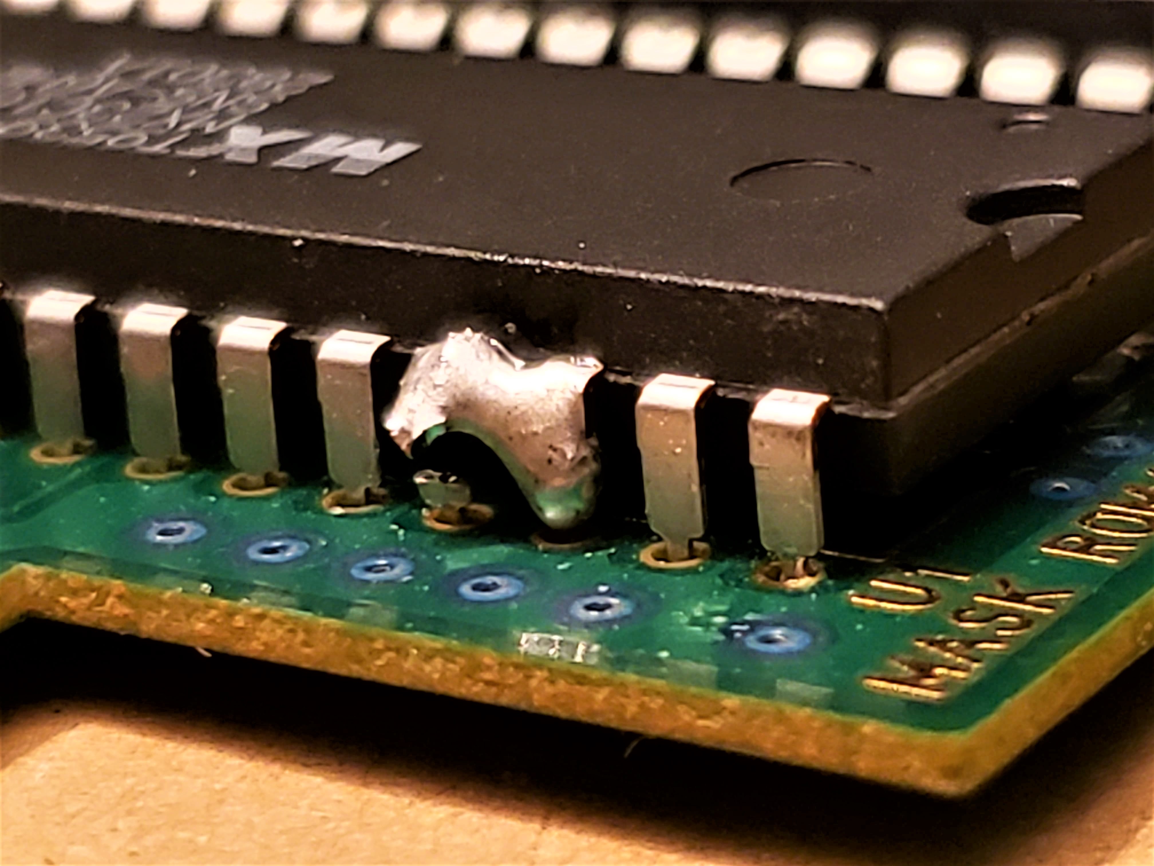
Now, flip the board back over, and cut pin 33 on the original ROM as close to the PCB as possible. Carefully bend it out a bit to make sure it’s not connected to the socket anymore. Bridge the pin to pin 34 next to it using solder or a wire. Make sure it’s not connected to the original socket anymore! This is the /OE pin (output enable), and we’re connecting it to VCC. This disables the output of the original ROM, and therefore allows the other EPROM that you connect on the board to operate without creating bus conflicts with the original ROM.
If your original board had a 36-pin socket, but only a 32-pin EPROM in it, you’ll have to add some wires that go down through the donor PCB and into the adapter board. It’ll still work just fine. I find it easier to cut a longer piece of wire to fish through the (usually solder-filled) extra holes. Just cut off the wire you don’t use after you solder the wires in. Note that the board in this picture is an old version – everything on this post still applies to the new boards as well, so don’t sweat it.

If you’ve got one of the 322 adapters that need through-hole parts, then add them now. The 74’32 might not sit all the way flat on the board, due to interference with the original cartridge board. Not a big deal.

Note: It’s best practice to include the 74’32, but you might be able to make the game without it. In that case, solder bridge the pads within the footprint area of the 74’32. DO NOT BRIDGE THE PADS IF YOU ARE USING THE 74’32 CHIP.

If you’re using the most recent revision of the 27C160 boards, make sure you solder bridge the pin selection pads to the 36-pin configuration.

How to Use the Adapters (32-pin Socket)
Some 32-pin boards have a ‘139 decoder or perhaps a MAD-1 on them that only allows the first 8 Mbit of data to be accessed. The 32-pin socket was only ever able to carry up to 8 Mbits. So it is possible that the board can only use games that are up to that size, without modifying other parts of the board. But for games larger than 8 Mbits, I recommend sticking to the 36-pin variety.
The process for using this board is the same as for the 36-pin socket, however, you will need to add a few extra wires. Just follow all the instructions above, leaving the extra four holes on the adapter board (1, 2, 35, and 36) empty. Then, simply add a wire from empty holes 1 and 2 on the adapter to GND (pin 16 on the 32-pin socket).
Or, if you’re using the most recent 27C160 adapter board, make sure to solder bridge the pin selection pads to the 32-pin configuration. You don’t need to rewire anything in this case.
Then, you should be good to go!
How the Adapters Work
The 27C160 boards are pretty straightforward, so I won’t spend too much time explaining them here. It’s simply rerouting the pins from the SNES socket to the appropriate pin on the EPROM.

If you look at the table, you’ll notice the address pins are offset by one. This is because the 160 is a 16-bit device by default, but the SNES operates on an 8-bit data bus. If we put the EPROM into an 8-bit operating mode by typing the /BYTEVpp pin to GND, then the Q15 pin becomes the A0 pin for the 8-bit data bus. We can ignore the data pins between Q8 to Q14.
As for the 27C322, this needs a bit more explaining. If you look at the pinout of the 27C322, you’ll notice the data pins go from Q0 to Q15. That’s because this is a 16-bit EPROM, where each word is 16 bits instead of the 8 bits the SNES uses, like the 27C160 I just described. So the first address of the 322 contains the first TWO addresses the SNES will use, the first from Q0 to Q7 and the second from Q8 to Q15.
The problem with the 27C322 is that we cannot force it into an 8-bit operating mode, like we can for the 27C160. So we need to be a bit creative.
Let’s look at the TL866 programming window to see what I’m talking about. Compare the left window here, which is an 8-bit EPROM, with the 16-bit EPROM on the right. These numbers are in hexadecimal, or four binary bits. So you’ll see on the 8-bit bus two-digit hex numbers, while on the 16-bit bus you’ll see four-digit hex numbers.

Let’s use the first two addresses, which are 0x78 and 0x18, as an example. If on a 16-bit EPROM we read only D0 to D7 (0x78), we’re completely missing all the data on D8 to D15 (0x18) – with each increasing address request from the SNES, we’re skipping every other 8 bits segment. In effect, on a 16-bit EPROM, A0 from the SNES should point to the bottom half (A0 = 0) or top half (A0 = 1) of each word. And therefore, A1 from the SNES is acting like the 27C322’s A0 pin. So all we have to do is shift the address pins from the SNES one position – A1 on the SNES is connected to A0 on the 322, A2 on the SNES is connected to A1 on the 322, etc. Then, we use the A0 pin from the SNES to control which half of the 16-bit word we read from. We can do this using a multiplexer.
A multiplexer is a device that is essentially a digitally controlled selector switch. In our case, we need eight separate switches to change between two different data lines all at the same time. D0 on the SNES should either read D0 or D8 from the 322 EPROM, D1 on the SNES should either read D1 or D9 from the 322 EPROM, and so on. When A0 from the SNES is 0, the multiplexer will route D0 to D7 from the 322 to the SNES, and when A0 from the SNES is 1, the multiplexer will route D8 to D15 from the 322 to the SNES. Make sense?
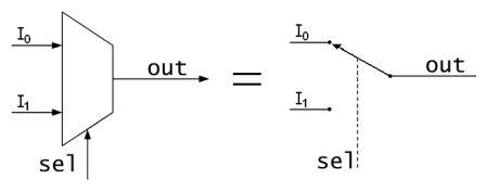
The 74HCT257 is a quad-package two-line multiplexer. If we use two of them in parallel, we can control all eight data lines. So, here’s how the EPROM connects to the multiplexers and the SNES Mask ROM pinout.
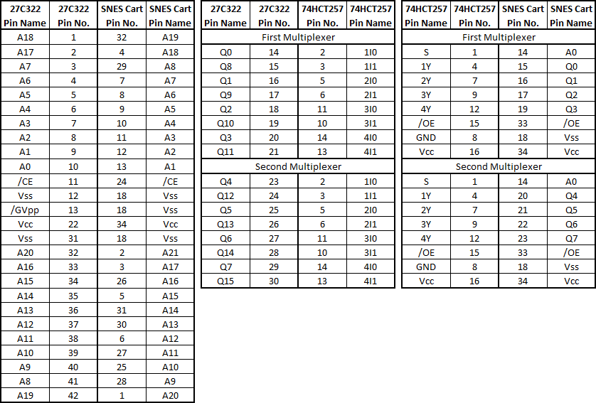
Finally, here’s the resulting schematic of the multiplexers. The rest of the pins on the EPROM go to the matching cartridge connector pin, but offset by one (A0 of the EPROM goes to A1 of the SNES cartridge connector, etc).


[…] with custom PCBs (to avoid destroying the ever-dwindling population of SNES cartridges) or a 27C322 or 27C160 adapter board on a donor cartridge. These larger EPROMs really make it easy to put your ROM on a cart, and using […]
LikeLike
So, I cut pin 34 instead of pin 33 on the mask rom by mistake. Repairing the pin is an option (although that could prove difficult). Is there another easier solution to fix my mistake? Can I just remove the mask rom completely?
LikeLike
No need to repair! Just leave pin 34 floating, don’t wire it to anything. Then take care of pin 33.
Tying pin 33 to VCC just disables the entire chip, instead of having to remove it. In truth you can accidentally cut any number of pins you want haha.
LikeLike
Thanks!
Alright, so I actually removed the mask rom completely 😀
I am still having problems with my repro cart unfortunately. I traced each 27C322 pin connection to the edge connectors and multiplexers and everything seems fine EXCEPT I cannot figure out where 27C322 pin 13 (GVpp) goes to. From reading your post, I figured it was connected to /CART but no dice. So, either I got a broken connection there or I am wrongly assuming that pin 13 is driven by /CART.
LikeLike
Pin 13 is just tied to GND, which permanently enables the ‘322 output. But, the multiplexers control the data bus output with their enable pins, that are connected to /CART. So the multiplexers act like a gate for the data to go out, and you don’t gotta mess with the ‘322 output logic.
If you want to send me some pictures you can, on my email, maybe I can see if there’s something wrong that way.
LikeLike
If my donor board has 2 32 PIN MASK ROMs (LoROM 8Mbit Donor Game Dennis The Menace) do I have to cut PIN 31 and tie to PIN 32 on BOTH MASK ROMS?
I haven’t been able to make your 27C160 Extended Board adapter to work with such a donor board.I have wired PIN 46 on the cartridge to PIN 42 of the 27C160 Chip but the game still doesn’t boot up. Do I need to do any special rewiring considering it’s two MASK ROMs in the donor board?
LikeLike
The adapter boards are specifically for single-ROM only games. Maybe I should be more explicit about that. What board type are you using? SHVC-something.
Also, is your ROM 16 Mbit? I think we can do some rewiring. The problem is the bottom ROM socket only provides the first 8 Mbit of memory. The second socket provides the second 8 Mbit. So you’re only loading half the game.
But yes as a first step you will need to cut both Mask ROM pins 31 and tie them to 32.
LikeLike
“the multiplexers control the data bus output with their enable pins, that are connected to /CART. ”
When I look at your picture, I see that it’s connected to /OE
LikeLike
Where are you reading that sentence from exactly? I can’t find it on this page anywhere, I don’t think I mention /CART at all.
/OE is pin 33 on the SNES Mask ROM socket, that’s where the mux enable pins are wired.
LikeLike
Would it not be a better option to pull Chip Select pin high instead of Output Enable on the original ROM? I doubt power is too much of an issue, but it provides greater overhead for additional hardware and/or bells and whistles.
The original ROM won’t be used, so deactivating it completely won’t pose an issue regarding speed. I suppose the CS pin isn’t right next to VCC, and that’s a slight inconvenience.
LikeLike
Made myself an earthbound repro no issues at all! Game boots fine and plays just like an authentic cart. But my main issue is that I have tried twice now to make a Chrono Trigger cart and nothing happens it just sits at a black screen… I was looking at the board and wondered if it may have something to do with the capacitors slots that are not populated??? Anyway great boards just not sure what I’m doing wrong… I’ve heard of possible anti-piracy measures but I’m using a japanese version of the game so the PCB is exactly identical. Any insight would be appriciated.
LikeLike
Earthbound and Chrono Trigger should be using the same board, and the boards in Super Famicom games are identical to the ones in US games, so there shouldn’t be any issue there. The adapter boards don’t require the capacitors to function, it’s just best practice to include them. I would guess you prepared the ROM incorrectly or there’s a solder bridge or a missing connection somewhere!
LikeLike
I’ve got a board with a 32-pin mask rom (SHVC-1A3B-12). How do I know if the adapter would work? This board has a 74LS139 decoder but I think that’s for the SRAM? According to SNES Central entry for this board, it supports ROM sizes up to 32Mbit, so it sounds like it should work? Since the ROM I want to burn is <16Mbit it's probably a better bet to use the 27C160 board?
Thanks for the help!
LikeLike
32 pin mask ROM means the original game is 8 Mbit maximum. To make something larger than that requires some custom rewiring that isn’t worth figuring out, and likely requires soldering to at least one cart edge pin. Highly suggest using a 36-pin donor, or a custom board
LikeLike