Please look at the main entry for more information on how to prepare the ROM file!
Here I will detail to you a quick and dirty guide to making SNES games using my basic custom boards. These boards are great for making simpler games, or transplanting working parts from any original SNES games that may be damaged in some way. There are two ROM socket types, but only one can be used at a time. This gives you the ability to:
- Make a game up to 1 MB (8 Mbit) using a 27C801 EPROM in the bottom set of sockets (note that ROM file must be swapbinned for use on the 27C801)
- Make a game up to 2 MB (16 Mbit) using a 27C160 EPROM in the top set of sockets
- Make a game up to 4 MB (32 Mbit) using a 29F032 + TSOP adapter board in the bottom set of sockets
- Make a game using a ROM chip from an original SNES board in the bottom set of sockets
This page will detail the hardware necessary for using the board in different modes – I will not be going over how to prepare the ROM file. You can view the main SNES tutorial to determine those details. And it is important to note, these boards cannot be used to replicate games that used specialty chips on their boards – this means you cannot make games that require: SuperFX, SuperFX2, DSP chips, SA-1, C4, S-DD1, or SPC7110.
Parts Needed (topside)
Here’s a breakdown of what parts you need based on what kind of game you’re making. All parts are located on the front of the board. For the discrete parts (resistors, capacitors, diodes, transistor) there are both surface mount pads and through-hole sockets available.

U3, U4 – EPROM or EEPROM
Needed for: Every game
Part Number: Bottom set – 27C801, 29F032 (plus adapter), or original Mask ROM; Top set – 27C160
Function: Holds the ROM file (use only one ROM chip)
How to Program: Check the reproduction article for more information (Steps 1, 5, 6, and 7)
C1 – Electrolytic Capacitor
Needed for: Games that save
Value: ~22 uF, at least 10 V rated
Example Part: Here is an example part from Digikey. Just make sure to get the right value and rating – note that if it is too tall, you might have to bend it down to sit flat on the board so it fits inside the cartridge.
Function: Prevents transient voltage drops on the SRAM during power-down.
CB – Electrolytic Capacitor
Needed for: Games that save
Value: ~22 uF, at least 10 V rated
Example Part: Same as C1.
Function: Prevents transient voltage drops on the SRAM during power-down.
C2, C3, C4 – Ceramic Capacitors
Needed for: Every game (only use C3 for 27C801/Mask ROM, only use C4 for 27C160)
Value: ~0.1 uF, at least 10 V rated
Example Part: Here is an example part from Digikey.
Function: Filters out high-frequency noise that can interrupt the function of the chips on the board
C5, C6 – Ceramic Capacitors
Needed for: Games that save
Value: ~0.1 uF, at least 10 V rated
Example Part: Same as C2-C4.
Function: Filters out high-frequency noise that can interrupt the function of the chips on the board
CIC – Region Lock-out Chip
Needed for: Every game (on un-modded SNES systems)
Part Number: 12F629, or the original CIC (only use one)
Function: Completes the region check with the SNES to let you play the game
Click here to jump to Step 9g of the main SNES tutorial to find out how to program the CIC, if yours isn’t pre-programmed
R1, D1, D2 – Resistors and Diodes
Needed for: Games that save
Value: 1 kΩ for R1, low reverse leakage diodes (BAT85 is suggested) for D1 and D2
Example Part: Here’s a resistor and diode from Digikey.
Function: Combines the battery and SNES voltage rails to power the SRAM and keep it working after the SNES power is turned off. To lengthen save data retention, it’s better to get diodes that have a low reverse leakage.
R3, R4, Q1 – Resistors and NPN Transistor
Needed for: Games that save
Value: 1 kΩ for R4, 10 kΩ for R3, 2N3904 for Q1
Example Part: Here’s a transistor from Digikey.
Function: Puts the SRAM into a low-power state during power-off.
R2, R5, D3 – Resistors and Diode
Needed for: Games that save
Value: 100 kΩ for R2, 10 kΩ for R5, low reverse leakage diodes (BAT85 is suggested) for D3
Example Part: Same as earlier parts.
Function: Adds save glitch protection. D3 keeps /RESET from staying high while the supply voltage drops. R2 is a pull-down resistor on the /RESET line. R5 stops erroneous operation of Q1 from leakage current out of U6 decoder.
R6, R7, Q2 – Resistors and NPN Transistor
Needed for: Games that utilize an AS6C1008 SRAM chip (U5)
Value: 100 kΩ for R6, 10 kΩ for R7, 2N3904 for Q2
Example Part: Same as earlier parts.
Function: Adds a load to the SRAM supply pin. There are protection diodes internal to the AS6C1008 (not present on other AS6C SRAM models) that causes noise to rectify onto the supply line. Because the load is too light, this voltage can float above the recommended operating limits for the chip. The circuit made by these three parts adds a small load to the supply to discharge the rectified noise. You do not need these parts if you are using an SRAM chip other than the AS6C1008.
B1 – Battery
Needed for: Games that save
Part Number: CR2032
Example Part: I commonly buy these pre-tabbed from eBay, but buying from Digikey or Mouser will probably give you higher quality longer-lasting batteries (be sure if you buy non-tabbed batteries to also get a battery holder – do not try soldering tabs onto batteries yourself).
Function: Keeps the SRAM on to retain data while power is off.
U5 – SRAM
Needed for: Games that save
Part Number: 6264 (64K), 62256 (256K), or 1008 (1024K) series SRAM (be sure to get low standby current model)
Example Part: If you have a choice, I recommend getting an SRAM chip as close to the amount you need. The AS6C1008 will be large enough for any game, but the AS6C62256 covers nearly all of them as well. The AS6C6264 works for games that have 64Kbit of SRAM, but they don’t work for multicarts (on my board). These SRAM chips also have a low data retention current, which is good for longer save battery life, but my tests show that generally the AS6C1008 has a higher data retention current than the AS6C62256 or the AS6C6264. A higher data retention current means your save data will be erased sooner (but should be safe for many years regardless). Also, as mentioned earlier, the AS6C1008 requires R6, R7, and Q2 to be included on the board. So you should stick to the 6264 or 62256 if possible.
Function: Holds save game data.
How to Determine Data Retention Current: If you have a multimeter, put it into DC millivolt mode and carefully measure across the terminals of R1. You should read a voltage somewhere in the single to fraction of a mV. Testing the chips I have in my stock, I usually read about 0.4 mV for 62256 SRAM chips and 1.6 mV for 1008 SRAM chips. You can calculate data retention current from this measurement with Ohm’s Law – V=IR. V (voltage) is this measurement on the multimeter, R is the resistance of R1 (1 kΩ) and I is the data retention current. So for the 62256 SRAM, I get a data retention current of 0.0000004 A, or 0.4 uA (microamps). For 1008 SRAM, I get 1.6 uA.
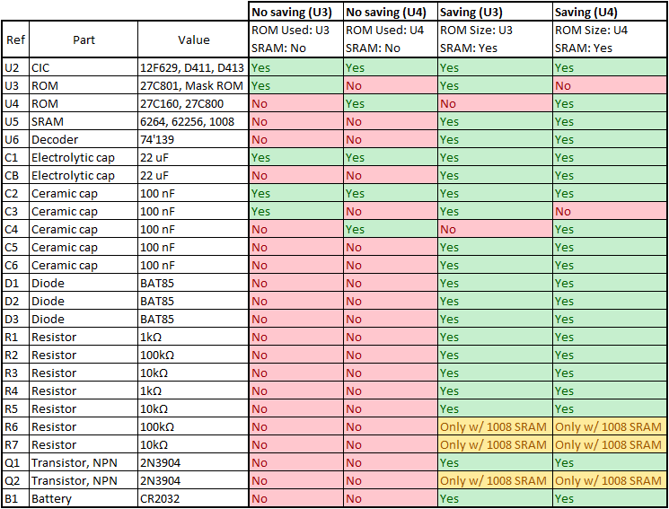
U6 – SRAM Decoder (middle of board, choose only one for LoROM or HiROM)
Needed for: Games that save
Part Number: 74HC139 (or equivalent)
Example Part: Digikey has many of the 74 series logic, but you might also be able to get them from TI directly.
Function: Activates the ROM or RAM, depending on the memory address being accessed. U6L is populated for LoROM games, U6H is populated for HiROM games. You can put parts in both sockets if you want, the board will still work.
Solder Pad (frontside)
There is only one set of solder pads on the front of the board.
Decoder Bypass
Shorted: Enables output on boards without SRAM or the SRAM decoder
Open: Does nothing (do not short unless you do not have an SRAM decoder)
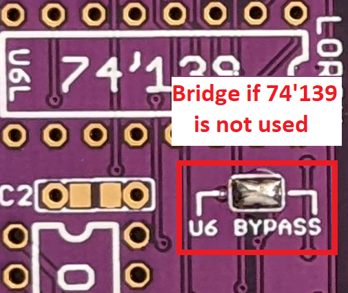
Solder Pads (backside)
There are a handful of solder pads you’ll need to bridge on the back of the board in order to make your game work.
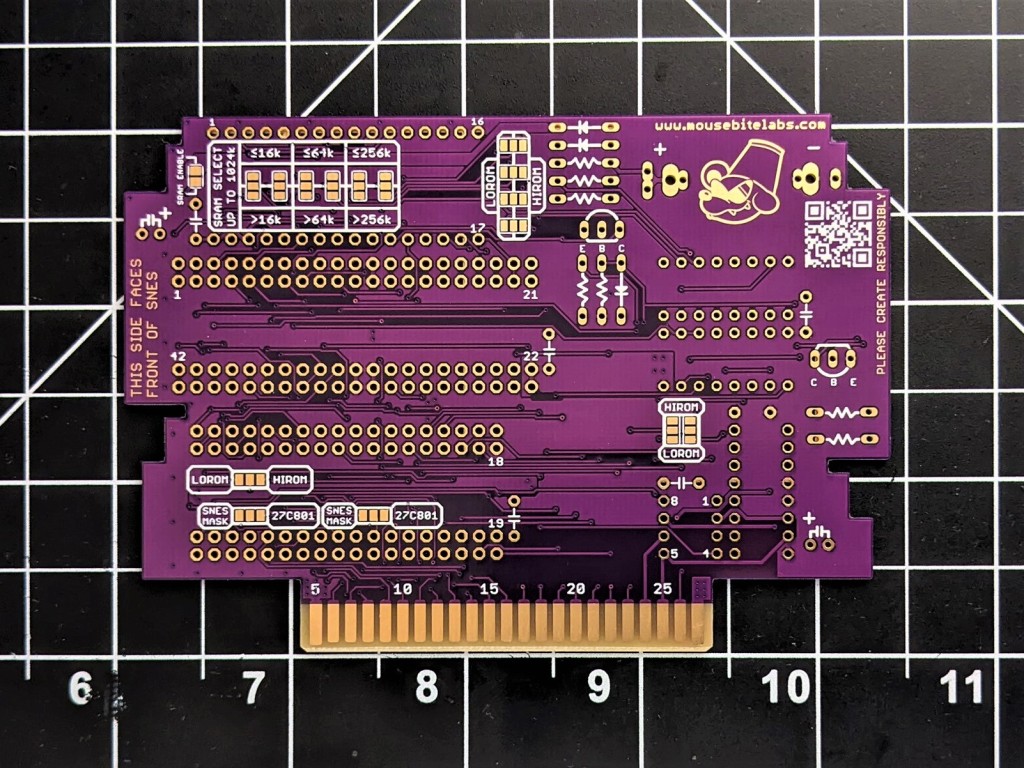
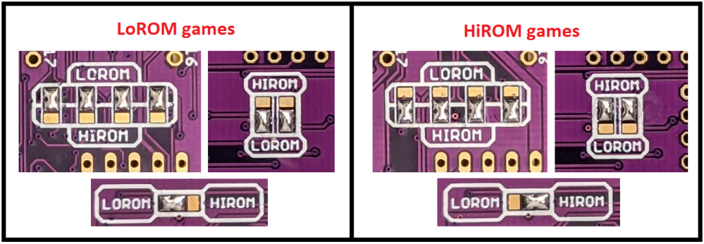
HiROM/LoROM Selection
There are a few sets of three-way solder pads located in various locations on the board. You need to bridge two of the three depending on what bank type your game is.
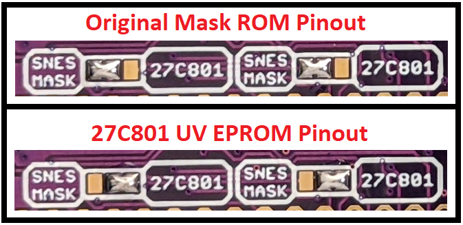
SNES Mask or 27C801 Selection
If you are using the bottom set of sockets, you need to solder these two sets of pads on the back to the type of chip you are using. If you are using the (swapbinned) 27C801, then solder the middle pads to the right; if you are using the original ROM or a 29F032/29F033 on a TSOP adapter board, solder the middle pads to the left.
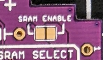
SRAM Enable
If you’re using SRAM, in the top left corner of the board bridge these pads together. If you reprogram your EPROM with a new game, you should disconnect these pads by desoldering them to reset the SRAM (they only need to be disconnected for a second). Then, resolder them together for your new game.
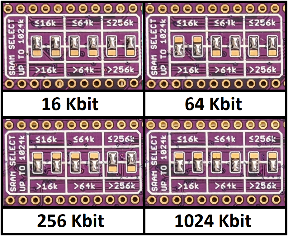
SRAM SIZE (SRAM selection pads)
These are another set of three-way solder pads, located in the top middle of the board. You need to bridge the set of pads (the middle and one to the top or bottom) depending on the size of the SRAM your game uses. Similar to the pads above, solder the two in the direction of the size of SRAM your game uses.

The prototype is well built and it will also give the best results.
LikeLike
Hi, can you guide me on which one is better tl866 or tl866ii?
LikeLike
Either works, though I think the ii is easier to find and has some more helpful error messages
LikeLike
For the 27C322 chip (do you sell the chip?) or something like this is ok? https://www.aliexpress.com/item/33013115995.html
LikeLike
I don’t sell the chips, but this is the exact model I use.
LikeLike
Great, thanks!
LikeLike
Can this somehow accommodate a 256k SRAM Chip?
LikeLike
No! Not without a few extra parts and ugly rewiring. But I ordered new boards that do support it natively! They have been delayed in shipping lately but they should be in pretty soon.
LikeLike
[…] Basic SNES Reproduction Board Guide […]
LikeLike
[…] Basic SNES Reproduction Board Guide […]
LikeLike
You say “R5 stops erroneous operation of Q1 from leakage current out of U8 ”
But there is no U8.
You may was talking about U5
LikeLike
Nice catch, thanks! That was copied from the Advanced board page, where the SRAM decoder is U8. It’s U5 on the Basic board.
LikeLike
**actually I meant U6, U5 is the SRAM
LikeLike